Dynamic Random Access Memory (DRAM) Cells
ABSTRACT
In this paper, I have provided an in-depth overview of dynamic random access memory. It discusses the DRAM basics, the architecture, and its use in circuitry. I have also reviewed the four, two, and one transistor DRAM cells. I have also used a control signal waveform to explain the Read and Write operations performed by various types of DRAMS. Also discussed in this paper is a comparison between DRAM and SRAM.
Keywords: DRAM, SRAM, DRAM Architecture, Circuitry
I. Introduction
While we can say that DRAM is a type of semiconductor memory, it doesn't operate the same way as other formats. Before you can design and use dynamic random access memory, you must understand its functionality and operations. The design and operation of DRAM are founded on MOS technology. This type of memory stores each bit of data using a capacitor. It also has a MOSFET, which is a transfer device, which acts as a switch. Whether a given bit is logical 1 or 0 depends on the extent of charge on the memory cell. If a charge is present in the capacitor then it is indicated by 1. On the other hand, if a charge is absent then it is indicated by 0.
In the past three decades, we have witnessed massive improvements in the performance of computer systems. This is all thanks to the evolution and advancement of silicon process technology which has led to the doubling of transistors on a single chip every other year (Moore’s Law). Also in this time, we have seen processor performance double because of increased switching speed and a bigger transistor budget. However, improvement in computer system performance for various types of applications did not result from an improvement in processor performance. This is because the performance of computer systems is limited by memory elements and the processor interaction. Additionally, unlike the rapid improvements that we have witnessed in the performance of processors, the performance of memory systems only boasts of modest improvements in the last three decades. As a result, modern computer systems have continued to be limited by the memory system's performance.
II. Literature Review on DRAM
A plethora of electronic applications uses dynamic random access memory. Despite being available in various sizes and packages, DRAMs essential have the same operation. The main purpose why DRAMs were designed is to store data. From elementary computer engineering courses, you must have learned that reading and refreshing data stored in a device is the primary purpose of a memory device. Several methods have been formulated to fine-tune the speed and efficiency of reading and writing memory. It is now more than 25 years ever since dynamic random access memory integrated circuits were developed. Dynamic random access memories have advanced from the archaic 1-kb(kilobit) generation to the modern 1-Gb(gigabit) generation. This was made possible with the evolution of circuit design and semiconductor technology. The feature and size of DRAMs have been massively reduced by the many advances in process technology. This has also allowed even higher levels of integration and major changes in component yield. As a result, the overall process solutions have remained not only competitive but also cost-effective. However, advancement in technology is not constrained to semiconductor processing. The numerous changes in process technology paved way for advancement in circuit design technology.
III. Dynamic Random Access Memory Architecture
Dynamic random access memory chips are big rectangular memory cells. These types of memory support logic and are mainly used to read and write data in arrays. DRAMs also guarantee the integrity of the data stored by refreshing circuitry.
Memory Arrays: These follow the pattern of rows and columns. This arrangement of memory cells is known as bit lines and word lines. Every memory cell is equipped with a distinct address. The location is defined by where the row and column intersect.
Memory Cells: As we already said, a dynamic random access memory cell is a charged capacitor that produces logical 1 or 0. Several designs have been considered over the years to help create memory cells on the chip. The trend today is the use of dielectric-filled trenches to develop the storage capacity element on the cells of the memory.
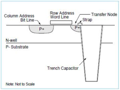
The figure above illustrates the IBM capacitor memory cell.
The Support Circuitry
The support circuitry of the memory chip allows you to perform various tasks such as reading the data that has been stored in the memory cells, writing to the memory cells, and refreshing the memory cells. The support circuitry, in general, has the following:
1. Amplifiers for sense: These amplify the detected charge or signal
2. Address logic: It is used to select columns and rows
3. RAS (Row Address Select) and CAS (Column Address Select) logic
4. Read and Write Circuitry: It supports the storage of information in the cells of the memory. It can also read the information that has been stored in the memory cells.
5. The internal registers and counters: Supports the tracking of the series of a refresh. It also initiates refresh cycles whenever needed.
6. Output: Ensures that logic prevents data from appearing
IV. The DRAM Circuits
Discussed below are some of the various types of DRAM cell’s circuits:
1. The Four-transistor DRAM Cell
The figure below illustrates the four-transistor DRAM Cell:
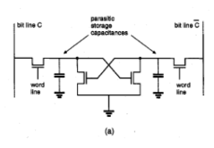
This is not only one of the first dynamic random access memory cells to be developed but also the simplest. It draws its design from the six-transistor static random access memory cell but without the load devices. The four-transistor cell boasts of two storage nodes, the diffusion capacitances, and the parasitic oxide. This type of cell does not provide a current path to the storage nodes to restore charge or signal that is lost due to leakage. For this reason, the cell must be periodically refreshed. Besides, this type of cell has only a marginal advantage over the six transistor SRAM cell.
2. The Three-transistor DRAM Cell
The diagram below is an illustration of the three-transistor DRAM cell:
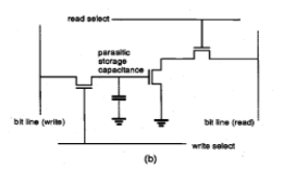
The three-transistor DRAM cell stores binary information in the parasitic node capacitance in the form of a charge. The charge stored in the parasitic node capacitance will determine whether the storage transistor turns on or off. The two-pass transistors support the reading and writing operations on data by acting as access switches. The three-transistor DRAM cell is known to have two different bit lines that are used for reading and writing data. This cell also has two different word lines that are in charge of the access transistor. The operations and the peripheral circuitry of the three-transistor dynamic random access memory cell are founded on the two-phase non-overlapping clock scheme.
3. The One-transistor DRAM Cell
The diagram below is an illustration of the one-transistor DRAM cell:
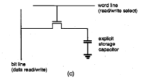
A one-transistor dynamic random access memory cell is made up of a single explicit capacitor for storage and a single access transistor. The storage capacitor is valued at 30-100 IF. Like in the three-transistor DRAM cell, the one-transistor DRAM cell also stores binary data with regards to whether data is present or absent in the storage capacitor. The word line is associated with a much bigger parasitic column capacitance. The operation of the 1-T DRAM cell greatly depends on the sharing of charge between the bigger parasitic column capacitance and the smallest storage capacitance. Also, this type of cell has a straightforward “data write” operation. For the write “1” operation, the write circuitry raises the bit line to logic “1”. The row address decoder also pulls high the selected word line. The storage capacitor is charged to a logic-high level when the access transistor is switched on. On the other hand, for the write “0” operation, the write circuitry raises the bit line to logic “0”. The row address decoder then pulls high the word line. We will have a result of a stored “0” bit when the storage capacitor loses charge via the access transistor.
A more elaborate read-refresh circuitry should be built if you want to read the data that has been stored in the one-transistor DRAM cell. This because of the notion that the “data read” operation in this type of DRAM cell is a destructive readout by necessity. Meaning, the data stored will be lost or destroyed during this operation. A typical "data read" operation begins with the column capacitance being pre-charged. To activate the access transistor, the word line is raised high. Charge sharing between the two capacitors will depend on the amount of stored charge in the parasitic column capacitance. As a result, we must refresh data every single time that a "data read" operation is performed. For example, a 256-cells-per-column DRAM read circuitry uses a cross-coupled dynamic latch circuit to restore signal levels and detect small voltage differences.
V. Read/Write Operations in DRAM
Maintaining effective read and write operations is very essential in DRAM. The other key issue is the noise immunity resulting from the charge capacitors voltages being small. I have mentioned below some of the lines that are used in the DRAM’s read and write operations:
1. Column Address Select (CAS)
The column address strobe selects the column that is to be addressed. The falling edge of the column address strobe line captures all the address inputs. Also, this line ensures that a column for reading or writing operations is chosen from the open row.
2. Output Enable
This signal supports the control of several memory chips that are in parallel. It takes care of the output that goes to the data input/output pins. When Row Address Select (RAS) and Column Address Select (CAS) are low, Output Enable is high and, Write Enable (WE) is low, the DRAM chip drives the data pins. It is possible to permanently connect Output Enable to low. This means that the output will always be enabled even if it is not required.
3. The Row Address Select (RAS)
From the word itself, it is easy to know that RAS selects the row that is to be addressed. Like in CAS, the falling edge of the RAS line captures the address inputs. As long as the row address select stays low, the selected row will be held open.
4. Write Enable (WE)
The write enable signal is used to determine if a particular falling edge of a column address strobe is a write or read. A low falling edge allows for the write action while a high falling edgeallows for the read action. The CAS’ falling edge will also capture the data inputs if low is enabled (write).
VI. Comparing DRAM and SRAM
Both static random access memory and dynamic random access memory are the basic classifications of RAM (Random Access Memory). RAM is usually a semiconductor device that is integrated into the chip that stores the processor. It is constantly used by the microcontroller to store variables used in calculations and other operations. The difference between DRAM and SRAM lies in their architecture. While dynamic random access memory used capacitors and transistors in an array of repeating circuits as we have already discussed, SRAM employs many transistors in a circuit to form one bit.
Static random access memory has no capacitors. The many transistors in SRAM are configured in a cross-coupled flip-flop. Also, unlike DRAM, SRAM does not need to be refreshed and is not constrained by the charge leakage issue. However, we will still need a constant supply of power in SRAM to keep that state of charge. As a result, both DRAM and SRAM are volatile. DRAM is considered cost-effective because it only uses a single capacitor and transistor per bit. The size, however, should not be compared because SRAM uses a different process than DRAM. The size will be based on the optimization goal that should be achieved. Moreover, SRAM is ten times faster than DRAM and is mostly used for cache. Dynamic random access memory, on the other hand, has a higher density and primarily used as the main processor memory.
Since SRAM is only made up of transistors, it only stores the binary bit in the form of voltage. The logical "1" is represented by 5V while "0" is represented by 0V. DRAM uses the absence or presence of a charge to store a binary bit. Logical "1" is represented by the presence of charge while "0" is represented by the absence of charge. This means that DRAMs need to be recharged or refreshed after 2 milliseconds because that is the time it takes for the capacitor to lose charge. For this reason, DRAMs are always equipped with a unique refreshing circuit. Although DRAMs are slower than SRAMs, they consume less power.
VII. Conclusion
In this paper, I have tried to dive deep and extensively explain the DRAM architecture and the circuitry of DRAM cells. Today, dynamic random access memory is popular and established in the technology arena. DRAM has become more reliable in expanding the memory of computer systems and other gadgets. While DRAM has its disadvantages, its pros in terms of cost, size, density, and satisfactory speed cannot be overlooked.